What Industries Commonly Use PCB Circuit Board?
Industries Commonly Use PCB Circuit Board
PCBs are the backbone of electronic products. They are the core of communication devices such as smartphones, tablets and computers, entertainment systems such as televisions and stereos, and home appliances including microwaves and coffee machines. Industrial equipment also relies on PCBs to function. These boards can be rigid or flexible, and can have copper traces and pads on either side. They can be single-sided or double-sided, or multi-layered, with several single-sided boards sandwiched together.
Rigid and flexible PCBs are used in a wide variety of industries, but the most important use is in consumer electronics. Consumers demand high-quality, reliable devices, and manufacturers must produce these products at a low cost to remain competitive. The industry also needs PCBs that can withstand the harsh environments they are exposed to, such as heat, moisture and physical force.
Traditionally, electronics were assembled from small integrated circuits and discrete components that were wired to each other on a rigid substrate, like bakelite or plywood. The system was difficult to debug and maintain, especially when large numbers of wires were involved, and reliability suffered. Modern pcb circuit board, which are much smaller and more dense, utilize a multi-layer base material, called a laminate or substrate, that has copper conductive pathways on one or both sides. The base material is usually a dielectric composite, consisting of a resin matrix with woven or non-woven glass fibers and filler such as ceramics. It is available in a number of different “flavors”, thicknesses and copper weights, offering mechanical support and specific electrical properties such as dielectric constant, temperature decomposition and arc resistance.
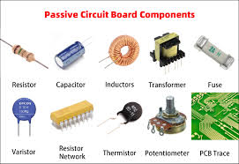
What Industries Commonly Use PCB Circuit Board?
Conductive paths on a PCB are routed with copper, and the surface of the board is coated with a layer of solder mask to protect them from damage or shorting during assembly. Holes through a PCB are drilled with computer-controlled drills, using a file that describes the location and size of each hole. Some holes are made conductive by electroplating the surfaces, and others connect layers of the board using hollow metal eyelets, known as vias.
All active electronic components need to be connected to power and ground planes, so they can send and receive signals. These signals are routed with traces, and the return path for these traces must be solid, so that noise doesn’t interfere with performance. Inconsistent or missing ground planes can degrade performance, and it is common to design these planes using a combination of techniques such as adding layers and cutting holes to create the necessary structure.
The final step of PCB manufacturing is etching the copper patterns on the surface of the base material. This is a process commonly known as photochemical etching. The pattern is exposed to light through a mask and then chemically developed, removing the unexposed film. This is followed by a coating of gold to improve signal transmission and corrosion resistance. Alternatively, the pattern may be electroplated on to a bare laminate using additive methods, or printed using photolithography.